- GCK - Global clock
- GTS - Global output enable
- GSR - Global set/reset CPLD control signals
2010년 3월 31일 수요일
What are GTS, GSR and GCK in Xilinx CPLD ?
Special globally routed nets (GCK, GTS, GSR) are faster and do not use function block resources.
2010년 3월 4일 목요일
ADC2USB
- Sampling Rate
- Main OSC
- The number of channel
- The number of sampling
- Components
CPLD(XC95144XL)
USB FIFO(CY7C68013A)
- Directories
Verilog HDL code to handle Xilinx CPLD
1.1.1. Inputs
* Reset - pin to intialize undefined variables from USB FIFO.
Note for testing CPLD, this pin is not abled,
because of USB FIFO module is not operated during CPLD test.
* Clk - clock pin to feed the 20 bits counter which is able to cover 20khz sampling with 8 channels
* Trigger - 8bits channel status pins to identify channels that need A/D conversion
* nEOC - end of conversion pin to confirm the completion of A/D conversion
* DB - 8bits data pins to contain A/D converted data
1.1.2. Ouput
* nCONVST - pin to confirm starting of A/D conversion
* A - 3bits address pins to select a A/D channel
* nRD - pin to confirm reading A/D converted data
* nSLWR - pin to confirm transferring A/D converted data to USB FIFO
* FD - 8bits data pins to contain A/D converted data to tranfer to USB FIFO
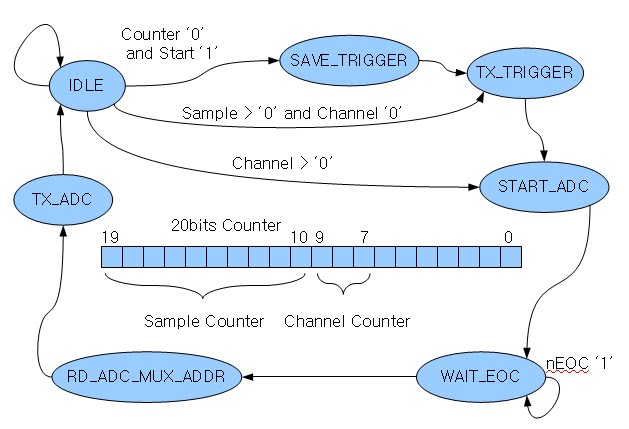
1.1.3. Counter
20bits Counter started by Trigger
* Sampling Count - position 19 to 10 bit, 10bits counter to count the sampling
* Channel Count - position 9 to 7 bit, 3bits counter to select the A/D channel
Note, for 20Mhz Clk, Channel Counter is ticked in 1/20us * 2^7 = 6.4us and Sampling Counter is ticked in 1/20us * 2^10= 51.2us (i.e. 19.53125Khz Sampling frequency)
1.1.4. State Machine
* IDLE - transite SAVE_TRIGGER or START_ADC according to the status of Counter
* SAVE_TRIGGER - save 8bits Tigger and transite to TX_TRIGGER immediately
* TX_TRIGGER - transfer the saved Trigger data to USB FIFO and transite to START_ADC
* START_ADC - activate nCONVST to start the A/D conversion and transite to WAIT_EOC
* WAIT_EOC - wait the completion of A/D conversion with low nEOC and transite to RD_ADC_MUX_ADDR
* RD_ADC_MUX_ADDR - read A/D converted data using nRD and DB and confirm next A/D channel to A pins
* TX_ADC - using nSLWR, transfer A/D converted data to USB FIFO
1.2. CypressFX2
USB FIFO Firmware of slave fifo, that have 8bits data bus, though Keil compiler
1.3. Driver
Libusb-Win32's USB Driver, library and run-time library
1.4. EggPort
PIC877a's Firmware through PIC-C compiler
1.5. SignalAnalizer
Application program through Visual C++ 6.0OutputsTriggered Status + 6bytes ADC data
피드 구독하기:
글 (Atom)